When the BE6502 computer is ready, it would be nice to connect it to a monitor. Luckily there are also some videos available from Ben Eater how to create a simple VGA adaptor. He calls it the world’s worst video card. For the analog output he created a simple 2bit digital analog converter (DAC) with two resistors per channel. This means he has implemented the 6-bit RGB mode. This can display 64 colors, which is more than the classic 8-bit computers could do. But still, I wanted to go for an 8-bit indexed mode, that is having 256 colors available from a larger palette.
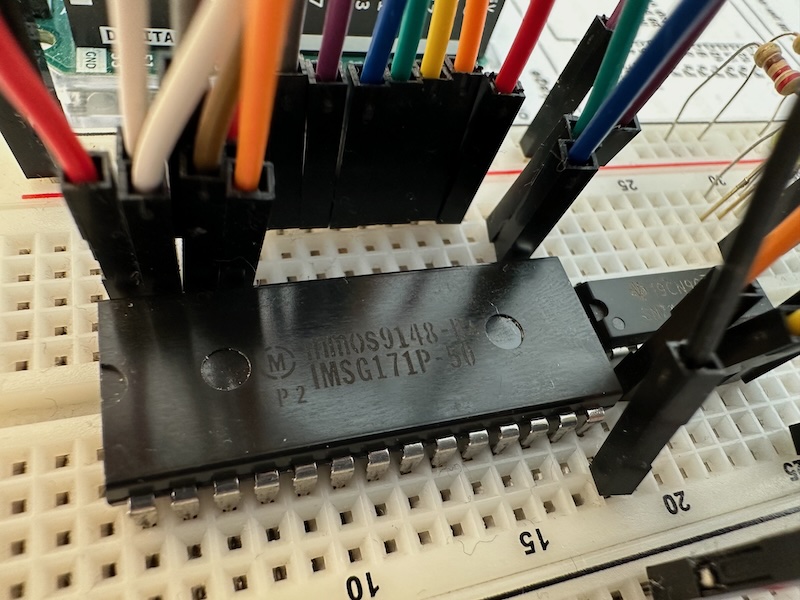
To do this one can use a later invention, called the RAMDAC. I managed to find an INMOS G171, one of the first such devices. The specification still calls it Color Look-Up Table (CLUT). It has an internal RAM for 256 18bit (3x6bit) entries and a 6bit DAC (see where the name RAMDAC comes from? 🙂 ) for each color channel. There are 8 input lines for the color index, you just put the color index on it (normally directly read from the video RAM), the G171 looks up the color in the internal RAM, and sets the R, G and B analog output through the DAC automatically. Additionally it has a so-called microprocessor interface to configure the palette.

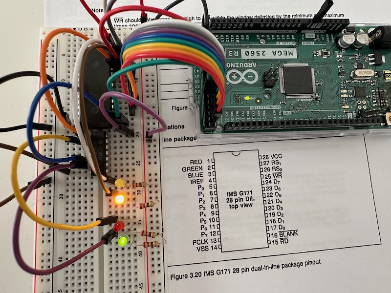
As the first step I wanted to check this interface that should work independently of the rest. This means, beside VCC (+5V) and VSS (GND) I just needed to connect these pins:
- WR* (25)
- RD* (15)
- RS0, RS1 (26, 27)
- D0 – D7 (17-24)
D0-D7 are input/output lines, the rest is input. To drive them, I have connected them to the Arduino Mega digital pins, and wrote a simple piece of SW. From the specification it looks like that the chip is not time critical, there are just some minima in the range of 10-100 ns defined, but no maxima, so I just put some ms delays between operations so that I can follow what is happening. I have also connected two yellow LEDs to RS0 and RS1, to see which register is being accessed and a red and a green LEDs to WR and RD to see the operations (this is done via an SN74LS04N inverter, because these two lines are active low).

The operation sequence is simple:
- Set RS1 and RS0 (
00– write mode address,11– read mode address,01– color value,10– pixel mask) - Pull WR down – this latches the register select
- Set D0-D7 to the data (address, color value or pixel mask)
- Pull WR to high – this stores the data
To read or write color values, first the address needs to be set and then three read/write operations to the color value register need to be done in the sequence of red, green and blue.
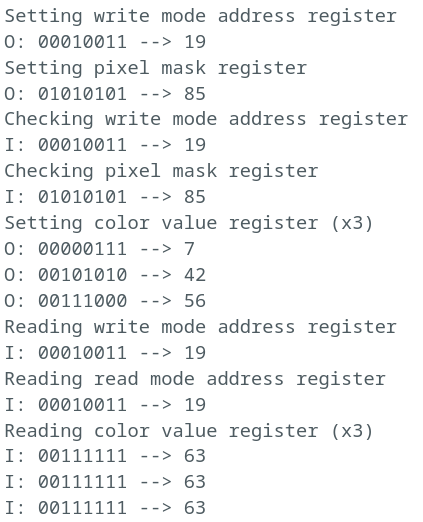
What I have managed so far is to set and read the address register and the pixel mask. Somehow changing the color value does not work. If I read out, it always gives 63 (111111). Furthermore after a color write operation the address is automatically changed so that the next entry can be written without the need to set the address again, but the address is not changed, so it looks like the write operation is not successful. Similarly during read the address is not increased either. But at least the other registers work, so this is a good sign.
