Fixing the RAMDAC

Yesterday I was unable to solve the issue with the RAMDAC not setting the color value register, so I gave up, and decided to make an entry about the progress so far. But I was so tired that I decided to do it this morning, making use of the public holiday. I was watching enough videos from Ben Eater by now to start suspecting the timing. Especially when I was trying to connect my clock module and sporadically the results randomly changed.

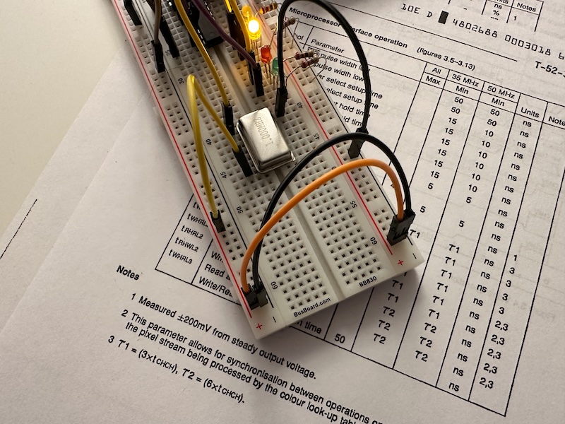
Today morning with fresh head, after creating the blog entry, I looked again into the G171 specification (as of today available for example here, or as part of the INMOS Graphics Databook here), and looked at the timings. The only difference I could see between the address register and the color value register was the minimal delay between address / color write and next read. For the address register it is tWHRL3, for the color value register it is tWHRL2. Timing between color value writes is tWHRL1. For tWHRL1 the minimum is defined as τ1, for tWHRL2 as well as for tWHRL3 it is τ2, where τ1=3 x tCHCH and τ2=6 x tCHCH. The value tCHCH is the time between two consecutive raising edges of the clock.

I decided to print out the data sheet, because I can think better if I can have it in my hand and make notes or drawings. But before looking into the papers I made some thoughts how I can insert a clock signal. First I was planning to use the Arduino, but I was not sure how to synchronize it with the other operations, and also I wasn’t sure if it was fast enough. Also I was not confident that my 555 based clock module can provide the right signal. And even though for most of the timings there are only minima and no maxima, the clock, that is tCHCH has a maximum: 10000ns. Note that the usual values are 28/20 for this chip, as it runs 35/50Mhz.

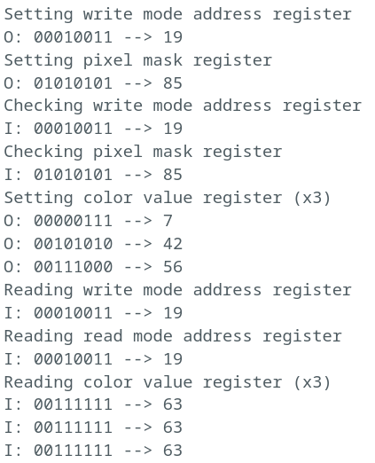
But, I happen to have two 1MHz quartz oscillators for the BE6502 project, and 1MHz means tCHCH of 1000ns, well within the range. And I expect it to be more stable than a SW clock from an Arduino. So I hooked up the oscillator, and connected it directly to pin with the lucky number 13, and tada… all read and write operations were working as expected.

Oscillator to the rescue

The data sheet does not explicitly describe this behavior, but it mentions that to enable independent access for the pixel interface and the microprocessor interface, the G171 internally synchronizes memory writes to the pixel clock.

Now the first step with the RAMDAC is done, I can move to the CRTC, but that is another story.

Playing with a RAMDAC

When the BE6502 computer is ready, it would be nice to connect it to a monitor. Luckily there are also some videos available from Ben Eater how to create a simple VGA adaptor. He calls it the world’s worst video card. For the analog output he created a simple 2bit digital analog converter (DAC) with two resistors per channel. This means he has implemented the 6-bit RGB mode. This can display 64 colors, which is more than the classic 8-bit computers could do. But still, I wanted to go for an 8-bit indexed mode, that is having 256 colors available from a larger palette.

To do this one can use a later invention, called the RAMDAC. I managed to find an INMOS G171, one of the first such devices. The specification still calls it Color Look-Up Table (CLUT). It has an internal RAM for 256 18bit (3x6bit) entries and a 6bit DAC (see where the name RAMDAC comes from? 🙂 ) for each color channel. There are 8 input lines for the color index, you just put the color index on it (normally directly read from the video RAM), the G171 looks up the color in the internal RAM, and sets the R, G and B analog output through the DAC automatically. Additionally it has a so-called microprocessor interface to configure the palette.

INOMS G171 – 50MHz variant

As the first step I wanted to check this interface that should work independently of the rest. This means, beside VCC (+5V) and VSS (GND) I just needed to connect these pins:

  • WR* (25)
  • RD* (15)
  • RS0, RS1 (26, 27)
  • D0 – D7 (17-24)

D0-D7 are input/output lines, the rest is input. To drive them, I have connected them to the Arduino Mega digital pins, and wrote a simple piece of SW. From the specification it looks like that the chip is not time critical, there are just some minima in the range of 10-100 ns defined, but no maxima, so I just put some ms delays between operations so that I can follow what is happening. I have also connected two yellow LEDs to RS0 and RS1, to see which register is being accessed and a red and a green LEDs to WR and RD to see the operations (this is done via an SN74LS04N inverter, because these two lines are active low).

G171 test setup

The operation sequence is simple:

  1. Set RS1 and RS0 (00 – write mode address, 11 – read mode address, 01 – color value, 10 – pixel mask)
  2. Pull WR down – this latches the register select
  3. Set D0-D7 to the data (address, color value or pixel mask)
  4. Pull WR to high – this stores the data

To read or write color values, first the address needs to be set and then three read/write operations to the color value register need to be done in the sequence of red, green and blue.

What I have managed so far is to set and read the address register and the pixel mask. Somehow changing the color value does not work. If I read out, it always gives 63 (111111). Furthermore after a color write operation the address is automatically changed so that the next entry can be written without the need to set the address again, but the address is not changed, so it looks like the write operation is not successful. Similarly during read the address is not increased either. But at least the other registers work, so this is a good sign.

Output from the test sequence