Adding ROM to the BE6502

It is nice to have a microprocessor that executes hard-wired NOPs, but if you want to do something more complicated then it is useful to have some kind of memory, for example a ROM. This is what also Ben Eater’s second video introduces for his breadboard computer. I already had an 32kByte EEPROM chip, just needed a programmer. And if you are building a breadboard computer and your wife understands what an EEPROM programmer is, then you can call yourself lucky. And if she buys you one then even luckier. :-*

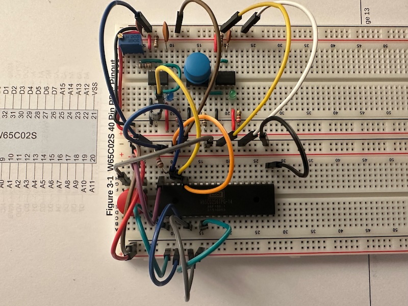
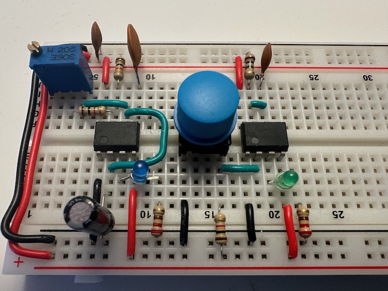
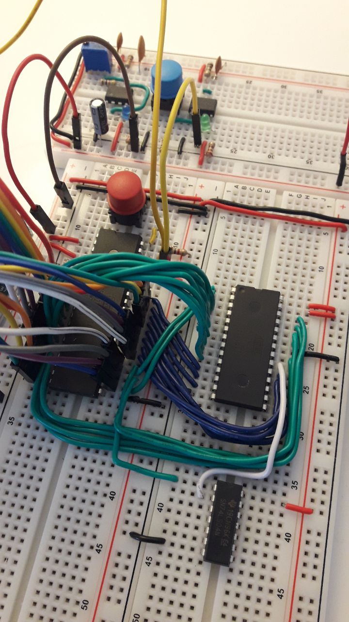
Connecting the EEPROM to the W65C02S is straightforward, you just have to look at the pinout carefully. The 6502 has the address bits on the “left” side top-down from A0 to A11, and on the “right” side bottom-up A12-15, and then the data bits from D7 down to D0. The AT28C256 on the “left” side starts on the top with A14, then A12 and then A7 down to A0. Then it has tree data bits D0 (aka I/O0) to D2 (I/O2). On the “right” side from the bottom D3 (I/O3) to D7 (I/O7), then chip enable, A10, output enable, A11, A9, A8 and A13. You can see in the picture below that the wires are a bit messy.

BE6502 with ROM

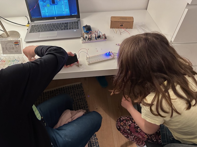
By the way, I have decided to use a different layout than Ben Eater: I plan to put the ROM and RAM chips to a breadboard above the CPU board, and later on the Versatile Interface Adapter (VIA) beside the CPU.

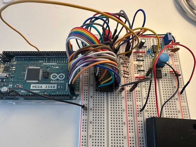
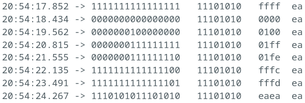
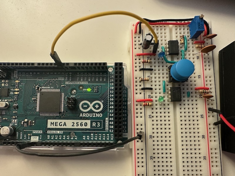
After putting in the wires, I have connected the arduino in place of the EEPROM to see if the wiring was correct. Afterwards I created the ROM image used by Ben Eater flashed on the EEPROM, inserted into its place. AAaaaand…. it almost worked. You can see the first 10 clock cycles below, 7 steps for reset, 2 for the read of the starting address and the last one is reading the first instruction.

Faulty output

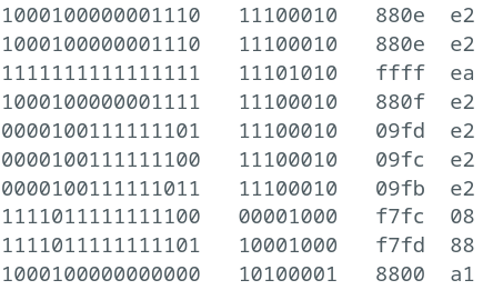
Reading the start address (reset vector) always happens from addresses 0xfffc and 0xfffd, so that’s where you can identify if something is wrong. As you see, somehow address bit nr. 11 was 0 instead of 1. But somehow the data has been read, although some bits were flipped there too. Anyway, first I looked at pin A11, it is easy to find, at the lower left corner of the CPU. I used colored jumper wires, they are in the sequence of red, orange, yellow, green, blue, purple, grey and white. A0 is red, A1 is orange, etc, and then A8 is red again, A9 is orange and so on. On the Arduino I used one row of the extra digital pins (22, 24, 26, … 52). Then the data pins are again D0 is red, D2 is orange, etc and on the Arduino they are in the other row of the additional pins, but only the upper eight (39, 41, 43, … 53).

And as it turned out, I mixed up two green wires! 44 went to D3 and 45 went to A12. This swap is best visible on these two lines, when fffc/00 is expected but f7fc/08 is shown. But, the good thing is that the board itself was ok, just the arduino was connected on the wrong way. After swapping back these two wires, everything was working as expected.

Small remark regarding minicom: if you use Debian, just download the source from git, build, create a .deb package and install. And it works.

Fixing the RAMDAC

Yesterday I was unable to solve the issue with the RAMDAC not setting the color value register, so I gave up, and decided to make an entry about the progress so far. But I was so tired that I decided to do it this morning, making use of the public holiday. I was watching enough videos from Ben Eater by now to start suspecting the timing. Especially when I was trying to connect my clock module and sporadically the results randomly changed.

Today morning with fresh head, after creating the blog entry, I looked again into the G171 specification (as of today available for example here, or as part of the INMOS Graphics Databook here), and looked at the timings. The only difference I could see between the address register and the color value register was the minimal delay between address / color write and next read. For the address register it is tWHRL3, for the color value register it is tWHRL2. Timing between color value writes is tWHRL1. For tWHRL1 the minimum is defined as τ1, for tWHRL2 as well as for tWHRL3 it is τ2, where τ1=3 x tCHCH and τ2=6 x tCHCH. The value tCHCH is the time between two consecutive raising edges of the clock.

I decided to print out the data sheet, because I can think better if I can have it in my hand and make notes or drawings. But before looking into the papers I made some thoughts how I can insert a clock signal. First I was planning to use the Arduino, but I was not sure how to synchronize it with the other operations, and also I wasn’t sure if it was fast enough. Also I was not confident that my 555 based clock module can provide the right signal. And even though for most of the timings there are only minima and no maxima, the clock, that is tCHCH has a maximum: 10000ns. Note that the usual values are 28/20 for this chip, as it runs 35/50Mhz.

But, I happen to have two 1MHz quartz oscillators for the BE6502 project, and 1MHz means tCHCH of 1000ns, well within the range. And I expect it to be more stable than a SW clock from an Arduino. So I hooked up the oscillator, and connected it directly to pin with the lucky number 13, and tada… all read and write operations were working as expected.

Oscillator to the rescue

The data sheet does not explicitly describe this behavior, but it mentions that to enable independent access for the pixel interface and the microprocessor interface, the G171 internally synchronizes memory writes to the pixel clock.

Now the first step with the RAMDAC is done, I can move to the CRTC, but that is another story.

Playing with a RAMDAC

When the BE6502 computer is ready, it would be nice to connect it to a monitor. Luckily there are also some videos available from Ben Eater how to create a simple VGA adaptor. He calls it the world’s worst video card. For the analog output he created a simple 2bit digital analog converter (DAC) with two resistors per channel. This means he has implemented the 6-bit RGB mode. This can display 64 colors, which is more than the classic 8-bit computers could do. But still, I wanted to go for an 8-bit indexed mode, that is having 256 colors available from a larger palette.

To do this one can use a later invention, called the RAMDAC. I managed to find an INMOS G171, one of the first such devices. The specification still calls it Color Look-Up Table (CLUT). It has an internal RAM for 256 18bit (3x6bit) entries and a 6bit DAC (see where the name RAMDAC comes from? 🙂 ) for each color channel. There are 8 input lines for the color index, you just put the color index on it (normally directly read from the video RAM), the G171 looks up the color in the internal RAM, and sets the R, G and B analog output through the DAC automatically. Additionally it has a so-called microprocessor interface to configure the palette.

INOMS G171 – 50MHz variant

As the first step I wanted to check this interface that should work independently of the rest. This means, beside VCC (+5V) and VSS (GND) I just needed to connect these pins:

  • WR* (25)
  • RD* (15)
  • RS0, RS1 (26, 27)
  • D0 – D7 (17-24)

D0-D7 are input/output lines, the rest is input. To drive them, I have connected them to the Arduino Mega digital pins, and wrote a simple piece of SW. From the specification it looks like that the chip is not time critical, there are just some minima in the range of 10-100 ns defined, but no maxima, so I just put some ms delays between operations so that I can follow what is happening. I have also connected two yellow LEDs to RS0 and RS1, to see which register is being accessed and a red and a green LEDs to WR and RD to see the operations (this is done via an SN74LS04N inverter, because these two lines are active low).

G171 test setup

The operation sequence is simple:

  1. Set RS1 and RS0 (00 – write mode address, 11 – read mode address, 01 – color value, 10 – pixel mask)
  2. Pull WR down – this latches the register select
  3. Set D0-D7 to the data (address, color value or pixel mask)
  4. Pull WR to high – this stores the data

To read or write color values, first the address needs to be set and then three read/write operations to the color value register need to be done in the sequence of red, green and blue.

What I have managed so far is to set and read the address register and the pixel mask. Somehow changing the color value does not work. If I read out, it always gives 63 (111111). Furthermore after a color write operation the address is automatically changed so that the next entry can be written without the need to set the address again, but the address is not changed, so it looks like the write operation is not successful. Similarly during read the address is not increased either. But at least the other registers work, so this is a good sign.

Output from the test sequence

Building the BE6502 computer – the microprocessor

As the very first step to build up the actual Ben Eater 6502 breadboard computer is to connect and power the 6502 microprocessor. Just like Ben Eater, we also got the modern variant of the 6502, the 65C02S from Western Design Center (WDC). This time it was my son who came to my help: he took a new breadboard, and following the video he attached the microprocessor and connected all the pins that needed to be connected, including +5V (VDD), GND (VSS) and the clock (PHI2). This is not a complicated setup, but of course one cannot really see what the processor is doing.

Connected 65C02S

To see what’s going on, I took the Arduino and connected all the address pins (A0-A15) and data pins (D0-D7) of the 65C02S to the extra digital IO ports of the Arduino.

Checking address and data lines with Arduino

With a small piece of SW as show in the video I could quickly see what was happening on the address and data buses. I mean almost… somehow the result didn’t match the one that Ben Eater got, but I quickly realized the root cause: he connected A15 through A0 to the even Ardunio ports 22-52, while I connected A0 thought A15. That is in the opposite order. But a quick change in the code fixed it. The final step was to add some resistors to connect the data pins and to hardcode the value 0xAE, so the output on the serial line was then just as expected:

Serial output of the address and data line monitoring

To hardcode the value, you take the binary value 10101110, and connect D7 through D0 with 1k resistors to +5V (1) or to GND (0). You can really read it off from the legs of the resistors as you can see the picture below. My daughter liked it so much that together we calculated how to change the configuration so that it shows 0x2A, because she is in class 2A 🙂

Resistors to hardcode data 0xAE, binary 11101010

Testing the Arduino

I already wanted to get an Arduino to do some experiments, but the final push was seeing Ben Eater using an Ardino Mega do do some debugging on his 6502 computer. Now that we have built up the astable and monostable timers and the Arduino also arrived it was time to test it.

The setup I used is quite simple: connect GND to the common ground, and pin 2 to the clock signal from the breadboard and then hook up an interrupt with pin 2 that prints out something. For the HW setup just two jumper wires are needed.

Arduino set up to monitor the clock signal

And the SW isn’t too complicated either.

#define CLOCK 2

unsigned int pushed;
unsigned long lasttime;

void setup() {
  Serial.begin(57600);
  Serial.println("Hello World");

  pushed = 0;

  pinMode(CLOCK, INPUT);
  attachInterrupt(digitalPinToInterrupt(CLOCK), onClock, RISING);
  
  lasttime = millis();
}

void onClock() {
  unsigned long time = millis();
  unsigned long delta = time-lasttime;
  lasttime = time;

  pushed = pushed + 1;

  Serial.print(delta);
  Serial.print("  You have pushed a button ");
  Serial.print(pushed);
  Serial.println(" times.");
}

void loop() {
  // put your main code here, to run repeatedly:
}

Monostable timer

Now that we have all the components, we have quickly built up the monostable time based on Ben Eater’s video. This time we build it up with my daughter, and Ludovicus the Lion also helped.

Ludovicus helping with the monostble timer

After the first prototype with jumper wires I have also cleaned up the board. On the picture you can also see the astable part that we cleaned up last time.

The cleaned up monostable timer

New package arrived

Finally I have managed to order some missing components for the Ben Eater 6502 breadboard computer.

Delivery box

Most importantly I have ordered a WDC 65C02, the newest CMOS version of the original MOS 6502 CPU. I have also ordered some tactile switches (push buttons). The old one was not stable enough and I have found the APEC MUTLIMEC 5G, which is quite robust, available in a through hole configuration, and the pins have a distance that is multiple of 0.1 inch, so they can be plugged into a breadboard. More precisely, the distance is 0.3 inches (7.62 mm), which is 0.1 inch (1 hole) bigger than some others I have seen in videos, but these are the ones that I could find in an online shop. The positive thing is that you can get nice button caps for them. I wish I could find some similar latching pushbutton or toggle swiches.

Two SRAMs, an EEPROM and a Versatile Interface Adapter (VIA) as well as an RS232 interface chip were in the package as well.

To be able to program and debug the setup I have also ordered an Arduino MEGA, with its 54 digital inputs I should be able to follow Ben Eater’s approach and see what’s happening on the various buses. And I can also experiment with other things using the Arduino. And I also ordered an Arduino Nano Every with headers. I just find it fascinating to have such a little board. And with the headers I can directly plug it into a breadboard.

Last, but not least, I have also ordered an LCD display. It was difficult to find one with direct interface to the controller chip. Most of them have a built-in SPI adaptor, so that it can be easily connected to a RPi or Arduino board without having to program the registers. But that’s not what I want to do.

Cleaning up the breadboard

Due to work and school we do not have much time for the electronics project, but we managed to get some wires and tools.

Tools and wires

The wires have the size 22 AWG, where AWG stands for American Wire Gauge. You can look up in the internet what sizes there are and what they mean in mm2. It took some time to find solid wires because sometimes it is not clear from the description if it is solid or stranded and the pictures often make things even more confusing. At the end I found the Haerkn Electric Wire Kit 22 AWG, solid, 7 colors. Product number B08BZKM7R5. So far I’m satisfied with it.

I got the tools from a local hardware store. Not the cheapest ones, but also not too fancy. I could not find a good stripper that also fits 22 AWG, so we got one that is adjustable with a help of a screw. Not perfect, but does its job. And here is a sentence I never thought I would tell to my son: “we are not going to give out 100 euro for a fancy stripper“. 😀

For hints and ideas we again turned to Ben Eater and his video, Breadboarding tips.

Both the kids were happy to help.

The kids with the tools

So far we managed to build up the astable 555 timer again, this time with fitting wires and tightly packed components. Unfortunately I forgot to take a picture of the board when it was finished, but you’ll see how it looks in the next post when we added the monostable timer.

Dual-boot

Note to self: after update sometimes Windows disappears from the grub boot menu. To put it back, just edit /etc/default/grub and add the line

GRUB_DISABLE_OS_PROBER = false

And then just run

# update-grub

That should put Windows back in the list. By the way, if os-prober is disabled, update-grub will warn you.

Railway crossing lights with the TLC555

After we successfully built a circuit to have a blinking green LED, we wanted to bring it to the next level.

First step: have alternating lights. It was quite easy, as we also had a Texas Instruments SN74LS04 inverter chip, we just connected it to 5V and GND, connected the output signal of the TLC555 to one of the inverters in the 74LS04 and got the inverted signal on the next pin, which then we could simply connect to another LED.

Next step: add a switch so select between stop (red) and go (white). No big thing, right? Add a switch, and then the output (clock) of the TLC555 can go to the red (as before) or to the white LED. Simple. And does not work. Remember the inverter? It inverts the input for the first red LED (red1) to get the signal for the second red LED (red2), so as soon as we switch on the white LED (white) the first red will be permanently off, so the second will be permanently on.

Luckily we also had the Texas Instruments SN74LS08 with 4 AND gates, so we could improve the logic. Put the switch to 5V instead of clock, and then AND the white state with the clock to get the white LED and the red state with the clock / inverted clock to get the two red LEDs. Basically the following:

white = go AND clock
red1  = stop AND clock
red2  = stop AND NOT clock 

It should work, right? Well, no. If the switch is set to go then the AND gate will get 5V plus the clock signal to get the white LED input, but if the switch is set to stop, then the go line will be open, and in this case the output of the AND gate is not defined.

To solve it, we turned around the switch: not to switch 5V between stop and go, but switch go between 5V and GND. This way go was always in a defined state, and to get stop we just inverted go. This way we get our nice railway crossing light.

Of course we have set it up with a bunch of control lights: two LEDs blinking alternately to show the clock signal, as well as an addition red and white LEDs to show the state of the switch.

breadboard with the railway crossing light simulator
completed circuit
schematics